Oops!

August 30th, 2006 by Adam

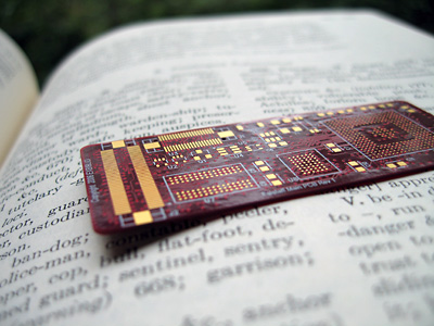
It was discovered yesterday that the SDRAM chip doesn’t fit in those beautiful red circuit boards we had delivered last week.

Turns out there was a mistake during the design process where an incorrect template was used for the SDRAM chip.

This will probably set the Falstaff project back about one week. The hardware team is continuing to assemble the other components to make sure that the rest of the design looks good before we have the board rebuilt.

Ian MacDuff explained that the team has taken a risk by shortening some of the more typical review processes because of our rapid 10-week prototype schedule. We hope that things go well and that we can have working prototypes much sooner than normal. However, if mistakes are not caught immediately (as in this case), it can delay the project.

Falstaff Software

August 29th, 2006 by Team Member

SpencerHi, This is Spencer Bliven. I’m a summer intern/part-time software engineer at Exbiblio. I thought I’d let you know about a part of Falstaff that I’ve been working on.

As the first hardware comes together, we on the software side have been hurrying to make sure that drivers and applications are in place so that the hardware can actually do something when it is finished.

There are a number of steps to go from a scan on the pen to text on your screen. First, the data must be transfered to your computer over USB. This can either happen right when you scan, if the pen is connected, or it can happen later when you next connect the pen to the computer.

The scans work by taking a series of small images as you drag the pen across the paper.

Best Conditions0000 Best Conditions0001 Best Conditions0002 Best Conditions0003 Best Conditions0004

This can be thought of as a video of what the pen sees, although it is at a very low frame rate. The next step towards extracting text is to stitch the small overlapping frames into one large image. We humorously call this process ‘storting,’ defined as the reverse of ‘distorting.’

David Warman has written a good program that takes the rotate, skewed, blotchy images we get from the pen and ‘storts’ them into a single image. The basic principle is the same as using Photoshop to stitch together several photos to form a panorama.

Stitched

After a single image has been produced we perform OCR (Optical Character Recognition) to convert it into text. This text is finally sent to the Life Library application as a capture: every pose, v

By Spencer Bliven

Falstaff Assembly

August 28th, 2006 by Adam

Brian Piquette (Synapse) and Ian MacDuff (Exbiblio) of our hardware team have provided the following photos of the bits and pieces of Falstaff coming together. Thanks guys!

Sensor Board: CMOS Image Sensor and Illumination LEDs.

This is the image sensor PCB. This PCB holds the CMOS sensor and the white illumination LEDs. It sits in the enclosure perpendicular to the long axis of the device, which points the sensor out the front of the unit.

Falstaff Assembly

Sensor Board with Lens Holder

The image below shows the sensor PCB with the milled plastic lens holder. The lens will screw into this plastic frame.

Falstaff Assembly

Sensor PCB mated with other PCBs in enclosure.

The PCB visible behind the Sensor PCB si the Main PCB. The Main PCB contains the processing core of the Falstaff unit. It has the ARM9 Processor, Flash and SDRAM.

Falstaff Assembly

Button PCB and Main PCB

The Button PCB (top) has the power supply, user interface (buttons and LEDs) and the interface between the sensor board and the main board.

Falstaff Assembly

Falstaff

August 25th, 2006 by Team Member

We’ve been using the name Falstaff to refer to our first prototype of the oPen. Falstaff will have three printed circuit boards (PCBs) to connect all of its electronic components: a processor board that has the processor, RAM, and ROM; an input/output board that has the buttons and lights; and an image-sensor board that, you guessed it, holds the image sensor and illumination lights.

Exbiblio Falstaff

Here’s a picture of Rev 1 of the Falstaff processor board which was completed on Wednesday. This board has eight layers of electrical connections through wires that are only 3 thousandths of an inch wide. The next step in the manufacturing process is to solder all the components onto this “bare” board.

Why isn’t this PCB green?

The color of a circuit board comes from the outer layer which is called a “solder mask.” The solder mask covers all the wires to protect them, but leaves holes where the components are soldered to the board. Without solder mask, PBCs are a dirty-yellow color. For some reason, most circuit boards are made with green solder mask, but the manufacturers have many colors to choose from. Since future revisions of this board may look very similar, it is handy to make each revision of the board a different color so that it is easy to tell them apart.

By Ian MacDuff

First Exbiblio Circuit Board

August 24th, 2006 by Adam

Exbiblio Falstaff Project

Hardware Demo at Company Lunch

August 2nd, 2006 by Adam

Ian 400
Dsc02420 400